 |
Tutorial on Guided-Wave Optics (TOM1) and Silicon Photonics (TOM2)
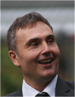
by Jean-Emmanuel Broquin IMEP-LAHC, Grenoble France
Description
Integrated Optics allows implementing on a single planar substrate many self-aligned optical functions. Based on a microelectronic-like realization process, these Photonic Integrated Circuits are today used in many areas ranging from Telecommunications to sensing via astronomy.
In this tutorial, we will present the fundamentals of guiding and we will explain the behaviour of elementary functions. Then, an overview of simple devices and their application will be provided. Finally, we will introduce the different kind of technologies that can be used to realize integrated optic devices. |
Biography
Jean-Emmanuel Broquin received an Engineering Degree in the Physics of Microelectronic devices from the Ecole Nationale Supérieure de Physique de Grenoble (France) in 1993, and a Master degree in Optics Electromagnetism and Optoelectronics from the Institut National Polytechnique de Grenoble (France) the same year. Since the completion of his PhD on Erbium-Doped Waveguide amplifiers in 1997, he has been working on both active and passive integrated optics devices (mainly realized on glass substrate). In 1999, he has been appointed Associate Professor at the Grenoble Institute of Technology (G-InP, France) and became a Full Professor in 2007. After having been in charge of the Photonics group of the IMEP (Institute for Microelectronics, Electromagnetism and Photonics), he is currently the Director of the IMEP-LaHC. Jean-Emmanuel Broquin has authored or coauthored several articles and conferences in the field of integrated optics devices, as well as patents. |
|
 |
Tutorial on Biophotonics and Medical Applications (TOM4)
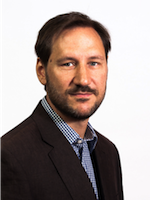
by Michael Pircher, Medical University Vienna Austria
Description
Optical coherence tomography (OCT) is a non-invasive optical imaging technology that provides cross sectional images of tissues with a depth resolution in the order of a few micrometer. There are many different applications for OCT ranging from biomedical imaging to material sciences. The main application of this technique, however, lies in the field of ophthalmology where it revolutionized diagnosis and treatment control. This tutorial will start with an overview of the historic development of OCT and introduces the underlying principles of OCT technology and different technical approaches such as time domain OCT, spectral domain OCT and swept source OCT. In addition extensions of the standard OCT technique including Doppler OCT or polarization sensitive OCT and their application for ophthalmic imaging are presented. |
Biography
Michael Pircher graduated from the Experimental Physics Department of the University of Technology of Graz, Austria in 2000. In 2003 he finished his PhD at the University of Technology of Vienna. From 2003 to 2006 he worked as a Postdoc at the Center for Biomedical Engineering and Physics of the Medical University of Vienna. From 2006 to 2012 he was working as an Assistant Professor at the Center for Medical Physics and Biomedical Engineering of the Medical University of Vienna where he gained his Habilitation in 2008. Currently he is Associate Professor and faculty member of the same department. His scientific interest lies in retinal imaging, adaptive optics, new contrast techniques in optical coherence tomography, coherence microscopy. |
|
 |
Tutorial on Nanostructured Materials for Photonic Crystal and Plasmonic Applications (TOM5)
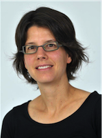
by Rachel Grange, Friedrich-Schiller-University Jena Germany
Description
Many innovations in medicine, optoelectronics or computer sciences rely on the development of new materials. Besides the well-established field of semiconductor electronics limited in speed due to electrical interconnects, dielectric photonics can reach higher velocity but is still limited in sizes due to the diffraction limit. More recently, the younger field of metallic nanostructures seems to be ideal to obtain higher speed and keep the size small, even though metal exhibits resistive losses due to its physical nature. This tutorial will review the fabrication processes and the outstanding electromagnetic properties of nanostructured materials like photonic bandgap crystal, metamaterials and plasmonics. We will show some recent applications offered by such artificial nanomaterials for manipulating the flow of light. |
Biography
Since 2011, Rachel Grange is leading a research group funded by the Carl Zeiss Foundation at the Institute of Applied Physics in the Friedrich Schiller University in Jena, Germany. Her research focuses on the synthesis, characterization and manipulation of semiconductor and oxides nanomaterials for nonlinear photonic applications and their combination with plasmonic structure to enhance the optical properties. Her main scientific areas include nonlinear optics at the nanoscale, nanomaterials as coherent biomarkers, niobate nanowires, core-shell nanoparticles, plasmonic structures for optofluidic applications and novel bioimaging techniques for deep tissue imaging. |
|
 |
Tutorial on Lens and look : optics in cinematography (TOM6)
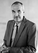
by Pr Peter C. Slansky, University of Television and Film, Munich Germany
Description
Movies are not about line pairs but about love affairs”. This bonmot illustrates, that lens design for cinematography has not only to deal with technical quality parameters like MTF, contrast and color rendition and so on but also with the “look”, that is created by the lens and other optical elements like filters in a certain scene, beyond the cadrage. In the workshop, the look parameters are explained and demonstrated with screenshots of scenes in comparison of different lenses from different manufacturers and of different age. A practical life demonstration with a camera and different lenses give a start to further tests by the participants. |
Biography
Prof. Dr.-Ing. Peter C. Slansky is executive professor for film and television technology at the Munich University of Television and Film (HFF), dean of studies of the HFF and vice chairman of the council of the HFF. He was born in 1961 in Krefeld. 1982 - 1984 Studies of machine engineering at the Duisburg University. 1985 - 1991 Studies of photo engineering at the University of Applied Sciences Cologne; Diploma in film- and television production techniques. 1992 - 1995 Studies of Audiovisual Media at the Academy of Media Arts Cologne; Diploma. 1988 – 1999 Freelancer filmmaker for corporate film and commercials. 1992 – 1999 Freelancer lecturer for film and television technology. Since 1982 photographer. Since 1993 author of books for film and television technology. Since 1999 executive Professor for film and television technology at the Munich University or Television and Film (HFF). Since 2005 founder/director of the Center for Advanced Studies of Film Technology of the HFF. 1999 – 2013 executive planner of the new building of the HFF (4 studios, 4 cinemas, > 50 postproduction rooms). 2013 PhD (Dr.-Ing.) at the faculty of Architecture of the Bauhaus-University Weimar about the planning process of educational buildings on the example of film schools. |
|
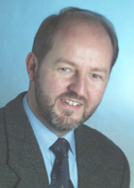 |
Tutorial on Organic Optoelectronics and Photonics (TOM7)
by Wolfgang Kowalsky Innovation GmbH, Heidelberg Germany
Description
Organic optoelectronics is based on evaporated or wet processed amorphous thin films of small molecules or polymers. Since there is no need for single crystal substrates this emerging technology allows the preparation of large area systems like emissive active-matrix displays, panels for lighting, and photovoltaic modules. In this tutorial, we will present the fundamentals processes in organic semiconductors like charge injection, transport, exciton formation and diffusion, and light absorption and emission. Then, an overview on applications on optoelectronic systems will be given by discussing the basic device structures and by summarizing the state of scientific and technical knowledge. |
Biography
Wolfgang Kowalsky was born in Erlangen, Germany, in 1958. He received the degree of Dipl-Ing., and the Dr.-Ing. and Dr.-Ing. habil. degrees in electrical engineering all from the Technical University of Braunschweig, Germany, in 1982, 1985, and 1989, respectively. In 1990 he was appointed Professor of Electrical Engineering at the University of Ulm, Germany. He has been Professor at the Technical University of Braunschweig and Head of the Institut für Hochfre¬quenztechnik since 1994. His current research interests are in the fields of organic semiconduc¬tors, light emitting diodes, photovoltaics, lasers, and organic-inorganic heterostructures. |
|
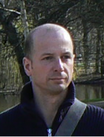 |
Tutorial on Optics Fabrication (TOM3)
by Oliver Fahnler, Fisba Optik, Switzerland
Description
To actually build well designed optical systems, it takes an optimum choice of existing fabrication technologies fulfilling all requirements concerning quality, batch sizes and production cost. This course adresses state-of-the-art fabrication technologies for modern optical systems focusing on the interference between optics design and optics fabrication. This course is based on an annual lecture on Optical Fabrication and Testing Technologies the speaker gives at the University of Delft. It focuses on glass processing especialliy the nature of grinding and polishing and their applications within various state-of-the-art Fabrication and Testing Techniques. From traditional optics shop grinding and polishing to aspheres generation applying cnc machinery to high end UPM grinding and CCP robot polishing applying dwell time based raster machining using various polishing techniques, e.g. Bonnet, EEM, IBF, MRF, PACE, FJP, Belt, Laser and grolishing. |
Biography
Oliver Fähnle received his PhD from Delft University in the Netherlands in Optics Fabrication and Testing and has been head of he Optics Fab Technology group at FISBA OPTIK in Switzerland ever since; he has been carrying out research in this field for more than 20 years seeking deeper insights in glass processing of Optical Elements – to be used for handling light in varous applications as a tool. |
|
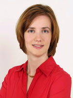 |
Tutorial on Utilizing Aspheres in Optical Design (TOM3)
by Ulrike Fuchs, Asphericon, Germany
Description
Aspheres are becoming more and more popular in optical design of lens systems. This trend is caused by the demand for reducing size and weight or even novel optical performance, which cannot be obtained with spherical designs only. This demand lead to innovative manufacturing processes for serial production of aspherical surfaces of high quality. Unfortunately, due to the type of surface form deviation introduced by CNC based grinding and polishing processes, tolerancing an optical system with aspherical surfaces becomes very complicated. Especially for serial production it is critical to know just how “good” an asphere has to be in order to guarantee the optical performance needed without overdoing it. Later one is a delicate issue to cost. This course will discuss how aspheres can be employed in optical design thoughtfully and how tolerances have to be dealt with. Special attention will be paid to surface form deviation and slope errors, which are unique to aspherical surfaces. |
Biography
Ulrike Fuchs studied physics at the Friedrich-Schiller University in Jena, majoring in optics in 2004. Her diploma thesis addressed ultrashort pulse propagation in complex optical system and optical design. Subsequently, she pursued her PhD in physics with a scholarship of the German National Academic Foundation at Fraunhofer IOF in Jena and received her PhD in 2009. Postdoctoral, Ulrike Fuchs worked as research associate at Fraunhofer IOF at the micro-optical department and as assistant lecturer at the Abbe School of Photonics. In 2010 she joined asphericon as optical designer and became head of department in 2012. Currently, she is involved in research and development at asphericon as well and therefore linking optical design directly to manufacturing processes and vice versa. |
|
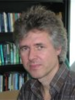 |
Tutorial on Adaptive Optics (TOM8)
by Michel Verhaegen TU Delft, Delft University of Technology, The Netherlands
Description
High resolution imaging with for example telescopes, microscopes or lithography machines is often hampered by the presence of dynamic wavefront aberrations. These dynamics have a spatial and temporal component and may be induced in various ways, such as due to turbulence or temperature gradients, etc. In this tutorial the basic components of a standard AO problem are reviewed followed by zooming in on the problems of wavefront reconstruction and feedback control design taking into account the wavefront dynamics. For wavefront reconstruction classical and novel types are reviewed based on the Hartmann-Shack sensor. For feedback control the relevance of taking the temporal dynamics into consideration is highlighted. We conclude with probing some future challenges. |
Biography
Michel Verhaegen is a professor in the Delft Center for Systems and Control of the Delft University of Technology since 2002. He has received various prestigious personal grant world-wide, such as from the US National Research Council, the Dutch Academy of Arts and Science and recently form the European Research Council. He is program director of the Dutch research program on Smart Optics Systems. This program that is running from 2008 to 2014 aims at developing integrated adaptive optics in various fields of applications ranging from Astronomy, microscopy to lithography. In 2014 he was elected research fellow from IFAC (the international federation of Automatic Control). |
|
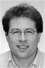 |
Tutorial on Finite-element Methods for Simulating Nano-optical Devices (TOM 9)
by Sven Burger, Zuse Institute Berlin & JCMwave, Germany
Description
State-of-the-art nanophotonic devices and materials are produced with sub-nanometer precision. Simulations of their optical properties are used for optimization and for a better understanding of their functionality. Further, in optical nano-metrology, numerical simulations are an essential part of the measurement and reconstruction process. In this tutorial basics of finite-element methods (FEM) for simulating Maxwell's equations will be introduced. Also, challenging applications with a specific focus on accuracy and speed of the simulations will be discussed. |
Biography
Sven Burger received a PhD from the University of Hannover, Germany. After a research stay at the European Laboratory for Nonlinear Spectroscopy, Florence, Italy, he joined the Computational Nanooptics group at the Zuse Institute Berlin, Germany. He also holds a position at JCMwave. Sven Burger's research interests include efficient numerical methods with applications to lithography, optical metrology, integrated optics, photo-voltaics, metamaterials, and plasmonics. |
|
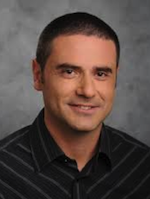 |
Tutorial on Ophtalmic Imaging Using Diffractive Optics (TOM10)
by Zeev Zalevsky Faculty of Engineering, Bar-Ilan University, Ramat-Gan Israel
Description
We will show several types of novel opthalmic devices such as contact lenses and intra ocular lenses which involve engraving of various spatial structures on top of the surface of those lenses. Those structures can have relatively large spatial features and then they are used to extend in an all optical way the depth of focus of those lenses in order to solve presbyopia and astigmatism problems. The structures can involve also small spatial features that aim to improve the modularity of the ophthalmic performance that those lenses have e.g. by preventing tears from covering those spatial structures and affecting the optical functionality of the lenses. Another type of spatial structures on top of contact lens that I will discuss will involve micrometric electrodes that are used in order to generate tactile electrically based stimulation of the cornea in order to allow blind users to "see" or to obtain some degree of spatial coordination and orientation. |
Biography
Zeev Zalevsky received his B.Sc. and direct Ph.D. degrees in electrical engineering from Tel-Aviv University in 1993 and 1996 respectively. Zeev is currently a full Professor in the faculty of engineering in Bar-Ilan University, Israel. His major fields of research are optical super resolution, biomedical optics, nano-photonics and electro-optical devices, RF photonics and beam shaping. Zeev has published more than 350 refereed journal papers, more than 190 conference proceeding papers, more than 315 international presentations, 32 issued patents and more than 15 patents pending, 6 authored books, 3 books as an editor and 27 book chapters. Zeev won various national and international awards such as the Krill prize, the International Commission of Optics (ICO) prize and Abbe medal, Juludan prize, the international SAOT Young Researcher Prize, the Lean and Maria Taubenblatt prize and the young investigator award in nanoscience and nanotechnology. |
